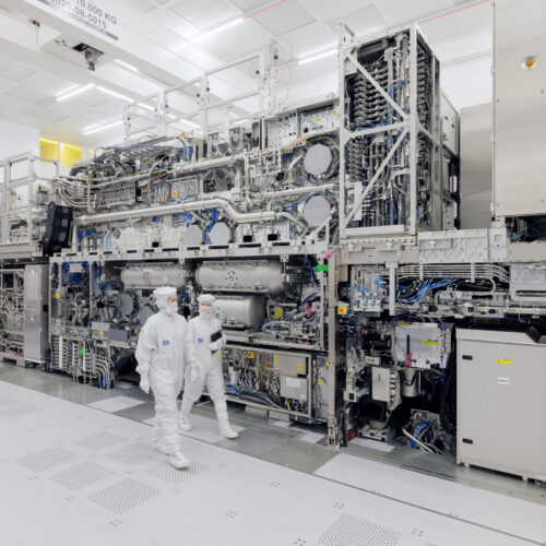
Chipmaking changes could boost productivity of new ASML machines by 40 percent.
By Nexvoro Tech Wire
PUBLISHED TUE, SEP 8, 2026 8:18 PM UTC • 6 MIN READ
Primary Journalistic Dispatch & Direct Reporting
Chipmaking changes could boost productivity of new ASML machines by 40 percent.
Leading chipmakers Samsung Electronics and Taiwan Semiconductor Manufacturing Co. announced plans to adopt ASML's latest chipmaking machines in the next several years - and they also joined Intel in agreeing to a crucial technology change that could boost chip production on the new machines by 40 percent.
This signifies the semiconductor industry's broader embrace of high NA EUV photolithography technology that can cost up to $400 million per machine and is only provided by the Dutch technology company ASML, Bloomberg reports . The technology would allow chip designers to implement even smaller features in potentially more powerful and efficient next-generation chips produced for AI data centers and consumer electronics such as smartphones, tablets, and laptops.
In-Depth Developments & Factual Context
ASML's EUV (extreme ultraviolet) lithography machines enable chipmakers to use powerful laser light to imprint patterns in silicon wafers, layer by layer, and gradually form the computer circuitry that makes silicon chips work. Compared to older deep ultraviolet lithography, EUV technology harnesses a more powerful source of light with a shorter wavelength to create even smaller features on silicon wafers.
This has necessitated development of an incredibly complex system of lasers that is continually zapping molten tin into plasma with temperatures around 200,000° C, along with mirrors collecting light from the plasma and redirecting it into a "bus-size" lithography tool for projecting the intricate circuitry patterns onto the silicon wafers, ASML researchers wrote for IEEE Spectrum . ASML's newest high-numerical-aperture (high NA) EUV machines use bigger mirrors and an improved optical system to more precisely collect and focus light.
South Korea's Samsung plans to use ASML's high NA EUV machines in producing memory chips by 2028. Meanwhile, Taiwan's TSMC aims to use the technology for manufacturing the most advanced chips for its customers - including companies like AMD, Apple, Nvidia, and Qualcomm - starting in 2030.
Industry Impact & Strategic Analysis
Intel has already begun adopting high-NA EUV machines in chip manufacturing. The US company has used the technology in high-volume manufacturing of Panther Lake processors for mobile computing devices starting in July 2026.
Samsung and TSMC are also now working with Intel and ASML to change the chipmaking standard for photomasks - the stencils that provide the intricate circuitry patterns imprinted onto silicon - from 6-inch photomasks to 12-inch photomasks. That shift could eventually improve the chipmaking productivity of high NA EUV machines by 40 percent, ASML chief technology officer Marco Pieters told Bloomberg.
The South Korean memory chipmaker SK Hynix is also considering joining the industry consortium overseeing the switch to the larger 12-inch photomasks, a spokesperson told Bloomberg. Like Samsung, SK Hynix is also aiming to start making memory chips using the high NA EUV technology starting in 2028.
Forward Outlook & Market Perspective
Improved production of chips has become a business imperative for as long as the AI bubble continues to inflate. Tech companies' rush to construct new AI data centers has also contributed to a global shortage of memory chips that has increased the prices of smartphones , laptops, and gaming machines .
Meanwhile, the importance of ASML machines for advanced chipmaking has also become a key issue in the ongoing tech competition between the United States and China . ASML still supplies Chinese companies like Semiconductor Manufacturing International Corporation (SMIC) with older-generation deep-ultraviolet lithography machines but has been blocked from exporting most of its chipmaking machines to China under Dutch government restrictions and US political pressure.
Despite unproven US government allegations that China managed to obtain one of ASML's EUV lithography machines, Chinese companies face an uphill battle in developing a homegrown version of the technology and the supply chain necessary to support production of such machines. An executive at Germany's Zeiss Group, the exclusive supplier of the mirrors and optical systems used in ASML machines, recently predicted that China would need 15 years to develop EUV lithography machines.
This story was updated on September 8, 2026, to correct the description of EUV technology in comparison with older technologies such as deep ultraviolet lithography.
Ars Technica has been separating the signal from
the noise for over 25 years. With our unique combination of
technical savvy and wide-ranging interest in the technological arts
and sciences, Ars is the trusted source in a sea of information. After
all, you don't need to know everything, only what's important.
Reporting synthesized and verified under Nexvoro.tech editorial guidelines. Full primary records referenced via Ars Technica.
Reporting synthesized under Nexvoro.tech Editorial Standards • Referenced via Ars Technica
Verified Dispatch